Toshiba Electronic Devices & Storage Corporation Launches 135°C-Rated Compact Photorelays for High-Temperature Automotive Applications
Toshiba Electronic Devices & Storage Corporation has announced the release of four advanced voltage-driven photorelays designed to meet the increasing thermal demands of modern automotive and industrial electronic systems. The newly introduced models—TLP3407SRB, TLP3412SRB, TLP3412SRHB, and TLP3412SRLB—are housed in the ultra-compact S-VSON4T package and are engineered to support a maximum operating temperature of 135°C. With volume shipments commencing immediately, these devices address the growing need for reliable switching solutions capable of sustained performance in high-temperature environments. The introduction reflects the company’s continued commitment to supporting next-generation automotive semiconductor testing and validation processes, where thermal stress conditions closely mirror real-world vehicle operating environments.
Rising Thermal Demands in Electrified and Autonomous Vehicle Systems
The rapid evolution of electrification technologies and autonomous driving systems has significantly increased the density and complexity of electronic components integrated into modern vehicles. Advanced driver assistance systems, battery management platforms, high-performance computing modules, and power control systems all require compact packaging solutions that maximize functionality within constrained spaces. As integration density rises, so too does the internal heat generated by semiconductor devices. Automotive semiconductors are now expected to function reliably at elevated temperatures for extended durations, reflecting real-world operating scenarios such as under-hood environments and high-load driving conditions. These developments have created a ripple effect throughout the semiconductor ecosystem, particularly in testing and validation infrastructure. Equipment used to evaluate automotive semiconductors—including testers, burn-in systems, and probe cards—must now operate under the same demanding thermal conditions as the components they assess. Consequently, every element within these systems, including photorelays, must maintain stable performance and electrical reliability at higher temperature thresholds.
Expanding Maximum Operating Temperature to 135°C
One of the defining features of the new photorelay series is the extension of maximum operating temperature from the conventional 125°C rating of previous products to 135°C. This advancement was achieved through careful optimization of the internal design architecture and refinement of the built-in elements within each device. By enhancing thermal tolerance at the structural and material levels, Toshiba has enabled these photorelays to maintain stable switching characteristics, insulation performance, and long-term reliability even when subjected to continuous exposure to high ambient temperatures. The 10-degree Celsius increase may appear incremental, but in high-density automotive semiconductor environments, such an enhancement represents a significant reliability margin. It allows equipment manufacturers to align more closely with stringent automotive testing standards and supports the accurate simulation of extreme operational conditions during component validation. This improvement ultimately contributes to greater confidence in semiconductor durability across the automotive supply chain.
Voltage-Driven Configuration with Integrated Input Resistors
Another major advantage of the new devices lies in their voltage-driven architecture, which incorporates built-in resistors on the input side. Traditional photorelay designs often require external input resistors, increasing component count and consuming additional board space. By integrating the resistor directly into the photorelay structure, Toshiba has simplified circuit design and eliminated the need for external resistor placement. This integrated approach offers multiple benefits, including reduced mounting area, simplified layout processes, and improved assembly efficiency. For designers working with high-density test boards or probe card assemblies, minimizing the number of discrete components is critical to maintaining compactness and signal integrity. The voltage-driven design also enhances usability by providing straightforward drive requirements, allowing engineers to integrate the photorelays more easily into a variety of testing and measurement circuits. This contributes to both system miniaturization and overall reliability improvements in high-temperature testing platforms.
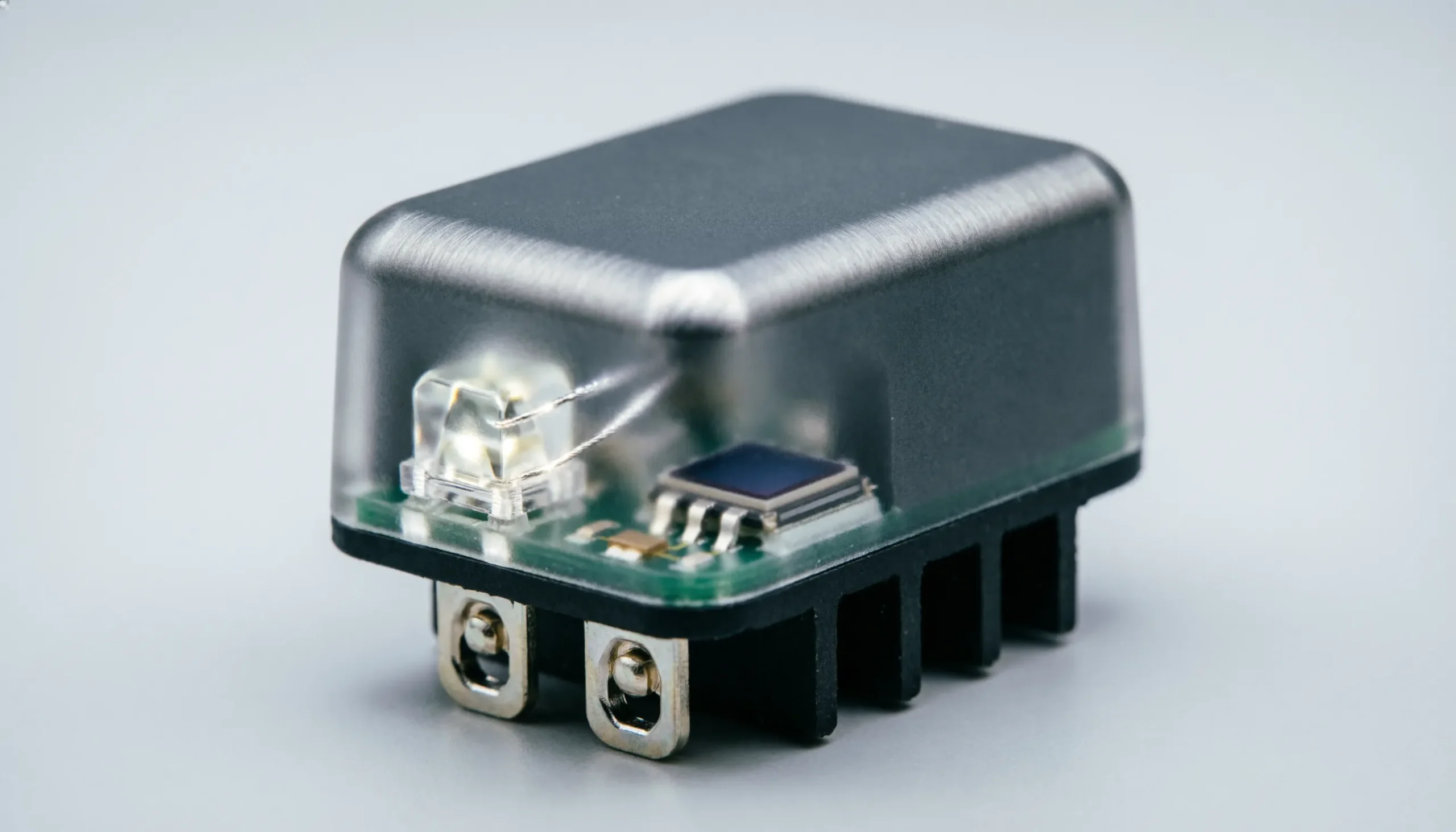
Ultra-Compact S-VSON4T Package for Space-Constrained Applications
Space efficiency remains a central challenge in modern electronic design, particularly within automotive semiconductor testing systems where numerous switching elements must be mounted on a single board. The new photorelays are housed in the S-VSON4T package, measuring approximately 1.45 mm by 2.0 mm in typical dimensions. This compact footprint enables designers to mount multiple devices within confined layouts without compromising performance or thermal stability. The small package size not only conserves valuable board space but also supports higher channel density in probe cards and burn-in systems. As semiconductor test environments become increasingly complex, the ability to integrate more switching elements within limited physical dimensions becomes essential. The S-VSON4T package addresses this requirement while maintaining mechanical robustness and thermal endurance suitable for high-temperature operation. The combination of compact packaging and enhanced temperature tolerance provides a powerful solution for next-generation semiconductor validation platforms.
Enabling High-Density Automotive Semiconductor Testing
Automotive semiconductor testers and burn-in systems frequently incorporate large arrays of photorelays to control signal routing and measurement paths during device evaluation. These systems must operate continuously at elevated temperatures to simulate real-world stress conditions. The new Toshiba photorelays are specifically engineered to meet these rigorous requirements. Their 135°C maximum operating temperature ensures consistent switching performance during prolonged thermal exposure, while their small size facilitates dense mounting configurations. Probe cards, which establish temporary electrical connections to semiconductor wafers during testing, also benefit from compact and thermally robust photorelays. Since probe cards often contain numerous channels within limited space, reducing component size without sacrificing reliability is essential. The integrated resistor design further enhances suitability for such applications by simplifying circuit construction and minimizing potential failure points. Together, these characteristics make the devices highly adaptable to advanced semiconductor testing infrastructure.
Supporting Reliability Evaluation in High-Temperature Environments
Reliability validation for automotive semiconductors involves rigorous stress testing, including extended operation at elevated temperatures to identify potential failure mechanisms. Burn-in equipment, in particular, subjects devices to prolonged high-temperature exposure to accelerate aging and reveal latent defects. Photorelays incorporated into these systems must maintain precise switching characteristics and insulation integrity throughout the testing cycle. The newly released models are engineered to withstand these demanding conditions, ensuring that the reliability evaluation process itself remains accurate and stable. By delivering consistent performance at 135°C, the photorelays help maintain signal accuracy and measurement consistency, contributing to dependable validation outcomes. This capability is especially important as vehicle systems increasingly rely on semiconductor components for safety-critical functions, including advanced driver assistance and electrified powertrains.
Enhancing System Efficiency and Design Flexibility
Beyond temperature resilience and compact dimensions, the new photorelays provide broader system-level advantages. The integrated resistor design streamlines printed circuit board layout and reduces assembly complexity, potentially lowering production costs and improving manufacturing throughput. The small footprint enables more flexible board arrangements, allowing designers to optimize signal routing and thermal distribution. In applications where multiple photorelays are required within a limited area, the cumulative space savings can be substantial. This efficiency supports the creation of more compact, lightweight testing systems capable of operating in temperature-controlled chambers or confined industrial environments. Additionally, the higher temperature rating offers greater headroom for engineers designing next-generation automotive semiconductor validation equipment, reducing concerns about thermal derating and improving long-term operational stability.
Meeting the Demands of Next-Generation Automotive Electronics
As the automotive industry continues its transformation toward electrified mobility and autonomous functionality, semiconductor devices will play an increasingly central role in vehicle architecture. Testing infrastructure must evolve in parallel to ensure the safety, reliability, and durability of these advanced components. Toshiba’s latest photorelay series represents a strategic response to these evolving requirements, combining enhanced thermal performance, compact packaging, and integrated functionality in a single solution. By pushing the maximum operating temperature to 135°C and adopting a voltage-driven configuration with built-in resistors, the company has addressed key design challenges faced by engineers developing automotive semiconductor testers and related equipment. The availability of volume shipments from launch further underscores readiness to support large-scale adoption.
The introduction of the photorelays marks a significant advancement in high-temperature switching solutions for automotive semiconductor testing applications. Through optimized internal design, Toshiba has extended maximum operating temperature capability to 135°C, exceeding the previous 125°C benchmark and aligning with the heightened demands of electrified and autonomous vehicle technologies. The integration of input resistors eliminates the need for external components, reducing board space requirements and simplifying system design. Encased in the compact S-VSON4T package measuring approximately 1.45 × 2.0 mm, these photorelays enable dense mounting configurations essential for probe cards, burn-in equipment, and advanced semiconductor testers. Collectively, these features position the new devices as a practical and forward-looking solution for engineers seeking reliable, space-efficient, and thermally robust photorelays capable of sustaining high-performance operation in demanding automotive and industrial environments.
Source Link:https://www.businesswire.com/